Technical Problem and Solution
demonstrated by Professor C. F. Quate’s groupP7P. However, this technique is limited to using conductive probes on very thin conducting photo-resists and the flexibility provided by DPN processes (choice of deposition and masking materials, ambient condition, and ease-of-use instrumentation) is not available with this approach. Microfabricated silicon nitride DPN pens that extend from linear arrays of writing pens (2 to 40 pens) to a one million parallel pen stamper prototype device (Figure 2) are available from commercial suppliers (e.g., NanoInk Inc.). Individual pens in a passive array do not write independently but are simultaneously brought into contact with the surface and moved together, allowing the duplication of a single pattern a number of times equal to the number of probes in the arrayP3, 6P.
B. Active Pen Arrays:
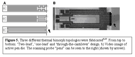
The passive pen arrays are limited to writing the same structure with all pens. This approach increases throughput n-fold with n pens if the desired final pattern is a repetition of the same sub-structure, spaced from each other by the probe pitch. For more complex and large-scale patterns, active pens are the enabling technology to use: if the actuated pens are spaced apart as far as the scanner area is across, the patterning area is effectively increased by a factor of n. If they are closer together, they have an overlapping area where multiple inks can be overlaid into a single writing space (i.e., the scanner range). The active pen arrays can be used to produce arbitrarily complex patterns of multiple inks over large areas. Individual pens can be actuated, or moved up and down using piezoelectric, capacitive, or thermoelectric actuationP9, 10P (Figure 3). The active pens were fabricated by thin-film deposition of heater elements on the SiN scanning probes using surface micromachining techniques forming a thermal bi-morph structure (RF-Sputtering of gold on SiN probes, lift off and wafer bonding). Resistive heating of the multilayer cantilever results in differential expansion of the components, leading to bending of the probe. Using this approach, a range of complex patterns can be generated at high speed because the contact between each pen and the writing surface is independently controlled by addressing each active pen with different electrical current signals at different frequencies and amplitudes – thereby controlling their individual motion. This results in a true “nano-plotter” capable of printing multiple colors (or chemical species) at desired locations.