|

Technical Problem and Solution
There are numerous needs for new materials, sensors and actuators that are required to enable the next generation of aircraft and spacecraft for defense, human spaceflight and for unmanned space missions. As described above the overall requirement for these devices is that they bring new capabilities coupled with significant reductions in mass, size and power consumption.
Scanning Probe Lithography has been proposed as the means to create these materials and devices at the nanoscale. Scanning Probe Lithography (SPL) is a novel technique for nano-fabrication with unique capabilities for highly scalable speed (parallel operation), enhanced resolution, and ultra-high registration of multiplexed molecular-scale bio-materials P1, 2, 3P
(Fig. 1)
Methods like e-beam lithography can provide high resolution and high-registration; however, e-beam lithography is slow, requires specialized resist chemistry and generally is incompatible with patterning large numbers of soft radiation sensitive bio-molecules. Methods such as stampingP4P and nanoimprinting- are powerful tools with high throughputs, and can operate in ambient environments; however, no existing stamping technology possesses the registration capabilities needed to |
|
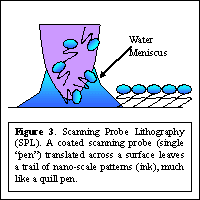 |
position different chemical and biochemical receptors at each individual site in an ultra-dense multiplexed nano-array. As perhaps the only lithographic technique that offers high resolution and multiplexed registration with parallel direct-write printing capabilities, SPL is a particularly attractive tool for patterning biological and soft organic structures onto surfaces. These molecules can be deposited in either ambient or inert environments without exposing them to ionizing UV or electron-beam radiation. Furthermore, several different kinds of molecules can be deposited without exposing the substrate to harsh solvents or chemical etchants, and without risking cross-contamination—the desired chemistry is carried out exactly, and only, where it is desired. |
|
|
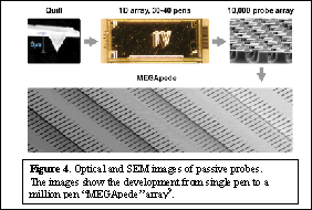
A. Passive Pen Arrays:
While retaining the ultra-high resolution and registration capabilities of the scanning-probe system around which it is based, SPL is especially amenable to high-throughput
“ parallel-pen ” fabrication strategies.P3, 6P Maskless lithography using scanning probe arrays has been |
| |
|
|
|
|